IBM Built a 100B-Transistor Chip. Five Years Is Fine
TL;DR - IBM crammed 100 billion transistors into something smaller than your fingernail using 3D nanostack tech. - That means 50% more oomph, or 70% less power drain versus their old 2nm nodes. - Training one LLM? Burns 284 tons of CO2. Roughly 125 round-trips JFK to PEK. - "Sub-1nm" describes vertical transistor height, not horizontal pitch. It's marketing with real physics underneath. - Data centers first. Edge devices later. Five-year horizon.
---
IBM dropped a press release last week that reads like a fever dream: a chip with 100 billion transistors at sub-1nm. The words "atomic-level engineering" appear. Twice.
Hacker News immediately called shenanigans on the naming, then spent three hours arguing whether the density math even checked out.
Standard behavior, honestly.
Here's what actually matters for your business.
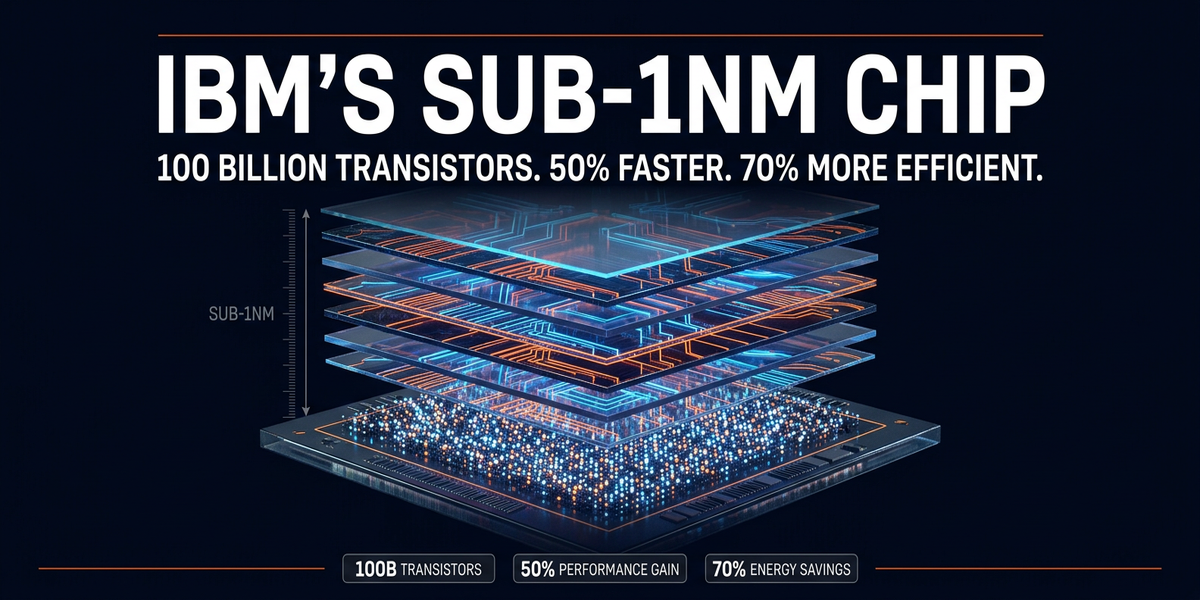
What IBM Actually Shipped
3D nanostack architecture.
Vertical transistor stacking instead of the flat-spread approach.
That vertical/horizontal split matters.
IBM's "sub-1nm" label? That's the vertical height of these little stacks. Horizontal pitch between them is still bigger than true 1nm. So yeah, marketing. One dimension, dressed up.
But the density gains aren't marketing.
IBM claims 50% performance lift or 70% energy savings versus their 2nm silicon. Cut those numbers in half if you want to account for the usual gap between announcement and actual silicon. You're still looking at a real jump in work-per-watt. The Hacker News engineers who actually tape out chips nodded at the density math. They rolled their eyes at the press release language. Both things can be true.
The naming is spin. The physics checks out.
Why AI's Power Bill Should Keep You Up at Night
284 tons of CO2.
That's what training a single large language model emits. Fun fact: that's roughly 125 round-trip flights between New York and Beijing.
Every API query you make burns a slice of that ongoing compute cost.
Right now, the model lives in some data center. You're paying per token.
The data center is paying for electricity, cooling, and hardware that depreciates the moment it ships.
Those costs flow back to you through token pricing, subscription tiers, and the occasional surprise invoice when traffic spikes.
Here's the thing though.
When chip efficiency improves — genuinely improves, not just on keynote slides — the cost to run the same inference drops. AI tool pricing is still tied to compute costs, which are tied to chip efficiency curves.
IBM's timeline is five years out. But the curve they're adding to has already dropped inference costs by orders of magnitude in the last three years.
No signs of that slowing.
You don't need to care about IBM specifically.
You need to care that the energy math keeping AI expensive is getting attacked from the hardware side. And it's starting to work.
What You Should Actually Do (Hint: It Isn't Waiting)
My agency runs AI tools for clients every single day.
We're not training models from scratch. Nobody small is. But we're querying APIs, serving outputs, running inference at scale. The compute bill is a real line item. Not the biggest one, but it grows as clients add features.
IBM's chip won't be in anything you can buy for five years.
First units go to hyperscalers, not to the edge devices your agency ships.
Here's the thing about technology curves though: they don't move straight. Inflection points tend to surprise you.
The real takeaway isn't "IBM has a magic chip." It's "the pressure on AI compute costs is real, sustained. And coming from multiple directions." Hardware efficiency. Better model architectures. Distillation techniques squeezing large models into tiny footprints.
Each one chips away at what you pay per query.
For shops running AI workflows today, the play isn't waiting for sub-1nm silicon.
It's auditing what you're currently spending on AI compute and asking whether your stack is optimized for the inference patterns you actually run. Most aren't. Most teams pick a tool, pay the sticker price, and never look at the invoice again.
That invoice is where the margin lives.
Side note: their press release is a mess. Buried the actual density numbers on page four.
The Trajectory Is the Point
IBM's announcement is real.
Five-year story. Sub-1nm label is marketing, but the density underneath it is legitimate.
What matters for your business isn't the chip. It's the curve.
AI compute costs have dropped dramatically. Will keep dropping. Which means the tools you're paying for today get cheaper to run tomorrow. And the tools you couldn't afford last year become viable this year.
The gap between "neat demo" and "profitable workflow" shrinks every time hardware efficiency ticks up.
Watch the curve.
Don't chase the announcement. And audit your compute bill before your vendor does.
---
Sources - IBM Newsroom: IBM debuts world's first sub-1 nanometer chip technology - Hacker News: IBM Sub-1nm Chip Discussion
Comments ()